Semiconductor and Electronics

Filter

Filters
Search

Showing all 14 results

  • Borer - Advanced Cleaning Solutions

    Borer – Advanced Cleaning Solutions

    Borer Chemie AG is a leading supplier of products and technologies for cleaning and disinfection. They develop, produce and market internationally known brand products and proven processes for professional applications in hospital hygiene, industr…

    Borer Chemie AG is a leading supplier of products and technologies for cleaning and disinfection. They develop, produce and market internationally known brand products and proven processes for professional applications in hospital hygiene, industry, laboratories and pharmaceutical sectors.

    Cleaning prior to coating, ophthalmic glass cleaning, flat panel display cleaning, laboratory glassware cleaning and instrument reprocessing are niches, in which Borer Chemie AG is successfully positioned. Services like cleaning validation and chemical analyses are further examples for the offered assistance by Borer Chemie AG.

  • Essemtec - Dispensing

    Essemtec – Dispensing

    Equipped with the most modern, accurate systems that drive and steering technology offers today. Mediums rarely behave the same way, environmental conditions are significant for the behavior of liquid changes. This is why there is virtually no sta…

    Equipped with the most modern, accurate systems that drive and steering technology offers today. Mediums rarely behave the same way, environmental conditions are significant for the behavior of liquid changes. This is why there is virtually no standard application in dispensing. Specific solutions for each dispensing task depending on both environmental influences and the type of liquid have to be evaluated. Easy programming and operation allow for a wide range of dispensing applications.

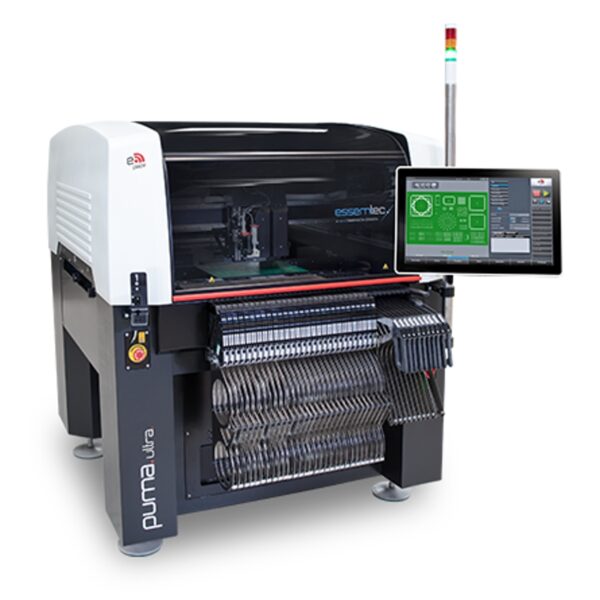
  • The Puma SMD Pick and Place with 280 Feeder. Adaptive modular machine concept with highspeed Mounting and Dispensing for ultraflexible, rapid prototyping and small series production.

    Essemtec – Pick-and-Place

    Designed for even more product changes per day, an even bigger range of components, increasing requirements for placement accuracy, speed and availability combined with high quality – naturally adaptive – engineering. Most feeders per sqm in t…

    Designed for even more product changes per day, an even bigger range of components, increasing requirements for placement accuracy, speed and availability combined with high quality – naturally adaptive – engineering. Most feeders per sqm in the marketplace, intelligent set-up concepts, the largest board sizes together with the most compact system sizes and the falcon software based on Essemtec`s “eez-technology“ ensure highly efficient and economical SMD manufacturing for service providers and in-house production.

  • PEER Group Equipment Automation Software for OEMs

    PEER Group Equipment Automation Software for OEMs

    PEER Group® provides the largest portfolio of equipment connectivity and automation software products to equipment makers (OEMs) in the semiconductor and related industries. With over 100,000 licenses shipped, PEER Group is the leading supplier o…

    PEER Group® provides the largest portfolio of equipment connectivity and automation software products to equipment makers (OEMs) in the semiconductor and related industries. With over 100,000 licenses shipped, PEER Group is the leading supplier of factory automation software for Smart Manufacturing and Industry 4.0.

  • PEER Group Factory Automation Software

    PEER Group Factory Automation Software

    PEER Group® provides the largest portfolio of factory automation software products and services to high-volume manufacturers in the semiconductor and related industries. With over 100,000 licenses shipped, PEER Group is the leading supplier of fa…

    PEER Group® provides the largest portfolio of factory automation software products and services to high-volume manufacturers in the semiconductor and related industries. With over 100,000 licenses shipped, PEER Group is the leading supplier of factory automation software for Smart Manufacturing and Industry 4.0.

  • SET - ACCµRA M

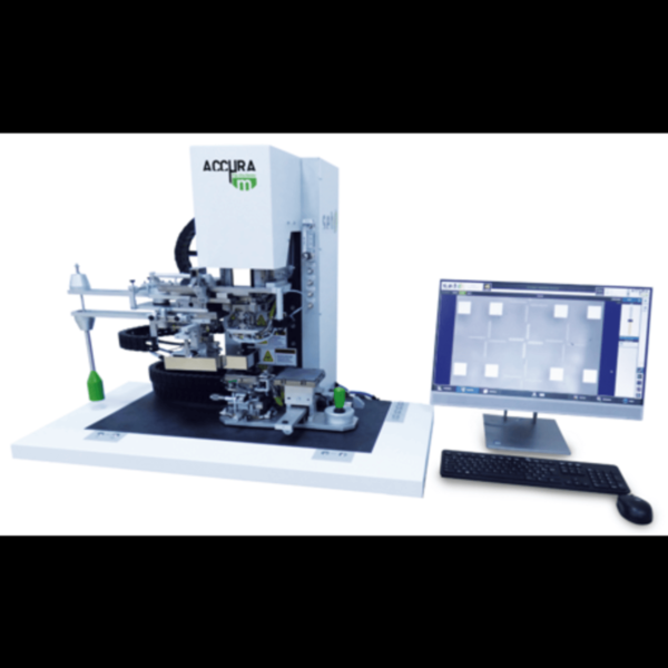
    SET – ACCµRA M

    The ACCµRA M is a manual flip-chip bonder that allows ± 3 µm accuracy. This equipment permits to align manually the components with a high level of precision. The motorized arm controls precisely the bonding force. Combining and synchronizing the arm with the temperature controller, it guarantees a perfect quality and high repeatability of your process. The ACCµRA M, more than a pick-and-place system, offers thermocompression and reflow capabilities. It is the perfect equipment for universities and R&D institutes.


  • SET - ACCµRA OPTO

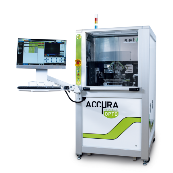
    SET – ACCµRA OPTO

    The ACCµRA OPTO is a flip-chip bonder that allows ± 0.5 µm accuracy. It is dedicated to low force and reflow processes. The ACCµRA OPTO combines high precision, flexibility and accessibility. It is the perfect equipment for optoelectronics an…

    The ACCµRA OPTO is a flip-chip bonder that allows ± 0.5 µm accuracy. It is dedicated to low force and reflow processes. The ACCµRA OPTO combines high precision, flexibility and accessibility. It is the perfect equipment for optoelectronics and silicon photonics applications.

  • SET - ACCµRA Plus

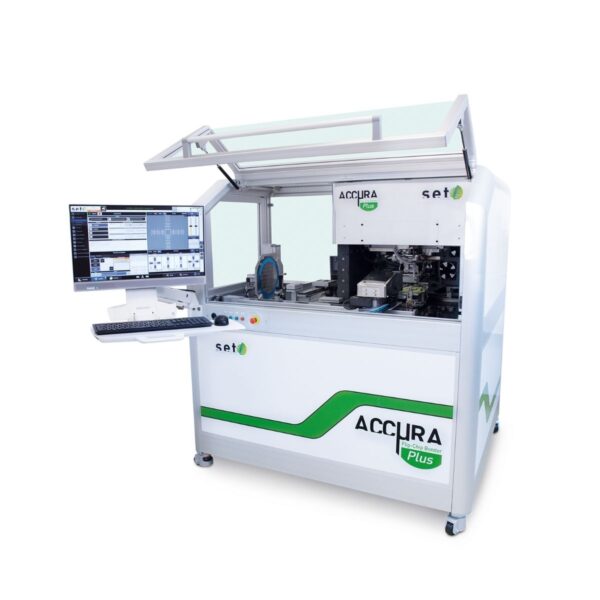
    SET – ACCµRA Plus

    ACCµRA Plus is a flip-chip bonder designed for ± 0.5 µm accuracy in full automatic mode. It is suitable for reflow and thermocompression processes.

    ACCµRA Plus combines high pr…

    ACCµRA Plus is a flip-chip bonder designed for ± 0.5 µm accuracy in full automatic mode. It is suitable for reflow and thermocompression processes.

    ACCµRA Plus combines high precision, flexibility and short cycle time. It is dedicated to production for Optoelectronic and Silicon photonics applications.

    Applications

    • Laser diode, laser bar
    • VCSEL, photo diode
    • LED
    • Prisms, lenses, mirrors
    • Micro Assembly
    • Flip-chip bonding, die bonding
    • Chip-to-chip, chip-to-substrate bonding

    Industries

    • Optoelectronics and Silicon Photonics
  • SET - ACCµRA100

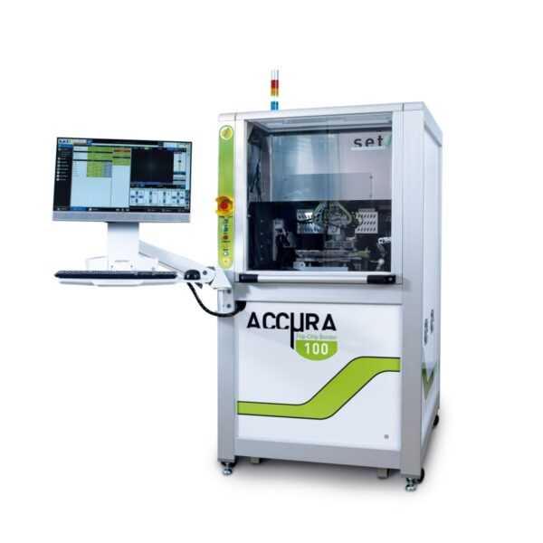
    SET – ACCµRA100

    The ACCµRA100 is a flip-chip bonder that allows ± 0.5 µm accuracy. Motorized axes guarantee a high repeatability of your process. Its flexibility makes it ideal for developing a wide range of applications. ACCµRA100 combines…

    The ACCµRA100 is a flip-chip bonder that allows ± 0.5 µm accuracy. Motorized axes guarantee a high repeatability of your process. Its flexibility makes it ideal for developing a wide range of applications. ACCµRA100 combines high precision, accessibility and cost-effectiveness. It is the perfect equipment for universities and R&D institutes.

    Applications

    • Micro assembly
    • Laser diode, laser bar
    • VCSEL, photo diode
    • LED
    • Flip-chip bonding, die bonding
    • Chip-to-chip, chip-to-substrate bonding
    • MOEMS, MEMS, MCM packaging…
    • 3D packaging
    • Nanoimprinting (UV NIL and Hot Embossing)

    Industries

    • Semiconductors
    • Memory
    • Optoelectronics and Silicon Photonics
    • Micro LEDs Displays
    • Quantum Computing
  • SET - FC150

    SET – FC150

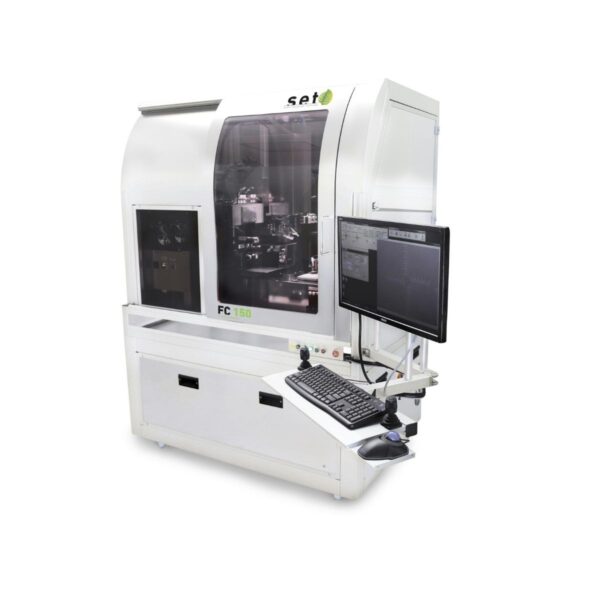
    The FC150 is an accurate and very flexible flip-chip bonder for Chip-to-Chip (up to 100 mm) and Chip-to-Wafer (up to 200 mm) applications on the same open platform.

    The versatile design and the possibility to combine different processes make the FC150 ideal for developing a wide range of assembly applications including focal plane arrays and optoelectronic devices.

    Perfect for advanced R&D, the FC150 is also appreciated for pilot production thanks to its full automatization.


  • SET - FC300

    SET – FC300

    The FC300 is a high accuracy and high force flip-chip bonder for Chip-to-Chip (up to 100 mm) and Chip-to-Wafer (up to 300 mm) applications. FC300 covers a large range of bonding forces, from 1 to 4000N. That makes it perfectly suitable for reflow and thermocompression processes.

    The leveling between both components is adjusted before each bonding within 1 µradian. The parallelism adjustment, the high resolution alignment and the perfect control of all bonding parameters allow to achieve submicronic post-bond accuracy.


  • SET - LDP150

    SET – LDP150

    The LDP150 is an electrical Press especially designed for bonding large light or radiation detectors (50 ~ 150mm). It uses compression process at room temperature (thermo-compression option available).

    …

    The LDP150 is an electrical Press especially designed for bonding large light or radiation detectors (50 ~ 150mm). It uses compression process at room temperature (thermo-compression option available).

    A predefined gap can be achieved between two components previously pre-bonded using a high accuracy device bonder such as the SET FC150. The devices are pressed together at room temperature while preserving the initial high accuracy alignment and parallelism.

    The LDP150 is able to apply pressure up to 100,000N.

    Applications

    • Large infrared focal plane arrays
    • Military and space applications
    • Large XY, UV detector
  • SET - NEO HB

    SET – NEO HB

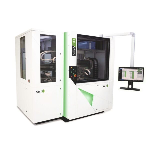
    NEO HB is a flip-chip bonder designed for ± 1 µm @ 3σ accuracy in stand-alone or full automatic mode (EFEM). It is suitable for Hybrid/Direct bonding processes. NEO HB combines high precision, flexibility and short cycle time…

    NEO HB is a flip-chip bonder designed for ± 1 µm @ 3σ accuracy in stand-alone or full automatic mode (EFEM). It is suitable for Hybrid/Direct bonding processes. NEO HB combines high precision, flexibility and short cycle time. It is dedicated for production.

    Applications

    • Hybrid / Direct bonding (room temperature)
    • Flip-chip bonding, die bonding
    • Chip-to-wafer, wafer level applications
    • Chip-to-substrate bonding
    • Pick & Place
    • Memory stacking
    • 3D IC
  • SET - NPS300

    SET – NPS300

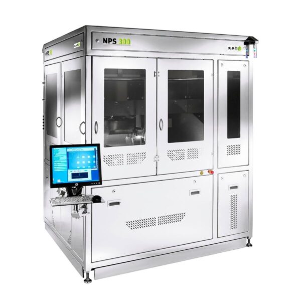
    Optimized for the production of nanostructures, the Nano imPrinting stepper Stepper NPS300 is the first ever tool able to combine Hot Embossing and UV-NIL on a same platform. The NPS300 is able to print sub-20 nm geometries with an overlay accuracy of 250 nm, when in-situ alignment is performed. Its flexible architecture offers an excellent process reproducibility and a unique ability to pattern large areas, in a sequential step and repeat mode on wafers up to 300 mm. It enables the low cost manufacturing of large stamps featuring repeated patterns.